


All Products
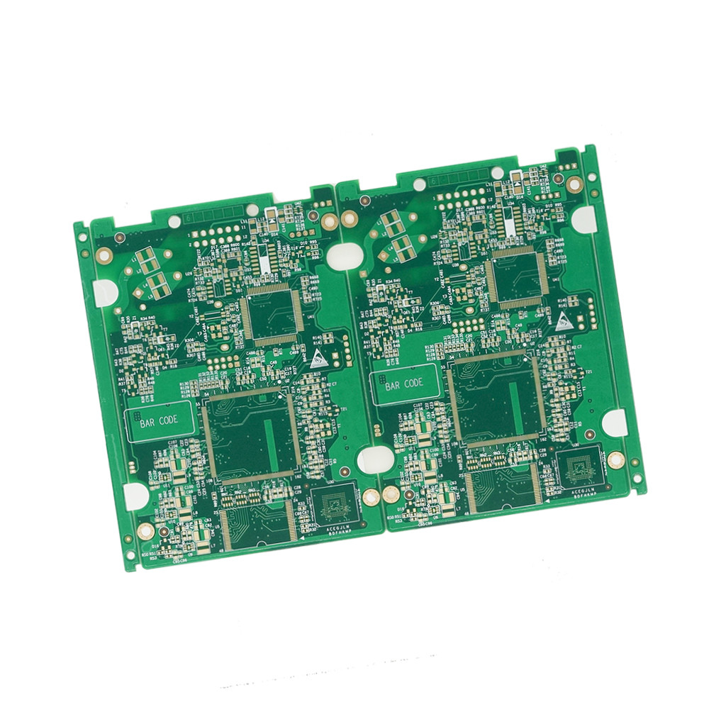
Advanced 22 Layer Electronic Circuit Board Design Custom Android Pcba Develop

| Place of Origin | China |
|---|---|
| Brand Name | CRT |
| Certification | ISO9001/ISO14001/IATF16949 |
| Model Number | CRT-SJ-010 |
| Minimum Order Quantity | 1piece |
| Price | US$ 1.18~2.73/piece |
| Packaging Details | Vacuum Packaging + Moisture + Humidity Card |
| Delivery Time | 14 working days |
| Payment Terms | T/T |
| Supply Ability | 40000sqm/month |
Product Details
| Application Segment | Auto, Industrial, Medical, DataCom, Camera | Layer Count | 1~22L |
|---|---|---|---|
| Matierial | PI, PET, PEN, FR4 | Board Thickness | 0.05mm~2.0mm |
| Copper Thickness | 0.33oz~6oz | Size | 3mm~1600mm |
| Highlight | 22 layer electronic circuit board design,advanced electronic circuit board design,android advanced pcb design |
||
Product Description
Shenzhen Custom Android PCBA Develop Design Service PCB Board Manufacturer
Advantages:
1) Professional engineer team --help you to check design and do engineering before production
2) Rich experiences in PCB production industry--provide high quality and competitive price PCB
3) After-sales service--every problem you have will get our professional advice and solution
4) Constant follow up-- make us have the fast reaction of your requirement
5) Inspected by the Inspection Institution
Specifications:
|
|||||||||||||||||||||||||||||||
Through Hole Assembly Capability:
Many high power, high reliability, and legacy products continue to be built with through hole components and Bandary will continue to serve these customers with Automated Axial Insertion, Hand Assembly, Wave Soldering, Selective Soldering, and Hand Soldering.
1. Universal Axial insertion
2. Terminal insertion
3. Custom Lead Forming Equipment
4. Pb & Pb Free Wave Solder
5. Selective Soldering
6. In-Line Continuous Depaneler
SMT Assembly Capability:
1. Panelized
2. Fine pitch and high count BGAs, Minimum package components(01005), POP, Chip on Board, RF microelectronics, press fit connectors, fiber optics.
3. Mixed processes (tin-lead and lead-free), lead-through holes, wave soldering , double-sided and single-sided reflow soldering, wide body and backplane.
4. Inspection and testing using online SPI ,online AOI ,X-Ray equipment.
Picture Details:
![]()
Recommended Products